This content originally appeared on DEV Community and was authored by Alex Esoposting
Two weeks ago I listed basic components necessary for building a simple computer, now it's time to design some of them. In this week's tutorial I'm going to design parts of the brainfuck computer that work outside of the BPU: memory and ways to communicate with the user. It will involve designing a flag circuit and learning a simple handshake protocol.
Memory
May contain knowledge
This is the most important part of the computer except from the CPU. It is used to store both a program the CPU runs and data it uses in it's computation. As a consequence a standard RAM chip will not require too much additional hardware to work with the BPU: the BPU will be designed to communicate with memory, not vice versa.
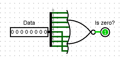
A memory chip is divided into cells which hold integer values, just like brainfuck memory. A BPU memory is connected to two buses: data bus, from which it will load and to which it will store it's contents, and address bus which selects a memory cell to interact with. To implement conditional jumps I also need a "Zero flag" line separate from the data bus which will check if the currently addressed memory cell is zero even if memory isn't broadcasting its contents to the data bus.
Memory will connect to following lines:
| Name | Type | Description |
|---|---|---|
| Address bus | Input | Used to address cells |
| Data bus | Input/Output | Used to communicate with other components |
| Zero flag | Output | Used by the BPU in conditional jumps |
D->RAM |
Control | Enables storing data from the data bus |
RAM->D |
Control | Enables loading data to the data bus |
| Reset | Control | Sets all cells to 0; connected to the computer's reset switch |
| Clock | Clock | Data is stored on rising edges of the clock if enabled with D->RAM |
Zero flag
Note that RAM->D doesn't connect to ld input of the RAM chip which would normally be used for this purpose. Instead ld is permanently set to 1 so that data is always broadcasted, but bridged off from the data bus by a buffer controlled by the RAM->D signal. This way it is possible to check if a cell is zero without broadcasting it's contents to the data bus. The small "=0" circuit which calculates the flag is just a single multi-input NOR gate.
Input/Output overview
Talking to other devices
Memory is only one of many circuits that a BPU might need to communicate with, but others don't get separate interfaces and signals: they all share the same lines and signals and may require an additional circuit to figure out which device the BPU is trying to communicate with.
Fortunately I will not need such a thing because I will only implement the simplest possible I/O for debugging and to show you the handshake protocol.
Handshake
The handshake is used when two devices (possibly running on different clocks so they are not synchronised) need to communicate. Except from any lines they need to send data two one-bit lines are required to perform a handshake: a "Start" flag controlled by the device that initialises the connection (the processor) and a "Ready" flag controlled by the other one (the device). The handshake proceeds as follows:
| Start | Ready | Description |
|---|---|---|
| 0 | 0 | The processor and the device are doing their separate things. When the processor wants to connect it broadcasts relevant data on the data lines, sets "Start" to 1 and waits. |
| 1 | 0 | When the device is ready it starts processing data broadcasted on the data lines. It may take any amount of time. The processor waits, still broadcasting data and setting "Start" to 1. After the device is done processing it broadcasts the answer, sets "Ready" to 1 and waits. |
| 1 | 1 | The device waits for the response. The processor captures data broadcasted by the device, stops broadcasting data and sets "Start" to 0 terminating the connection. |
| 0 | 1 | The device stops broadcasting data, sets "Ready" to 0 and continues it's operation until another communication is requested. |
This method has many advantages: it is simple, it assumes nothing about both devices and it allows for temporary synchronisation between components that can otherwise be running on very different speeds.
Handshaking in the BPU
Two Brainfuck Assembly Language commands are used for communication with external devices: , for input and . for output. They will perform a variant of the handshake described above.
For this purpose the BPU needs equivalents of "Start" and "Ready" signals that would also specify whether the processor requests an input or an output. I will implement this on three signal lines: in for requesting input, out for requesting output and resume as an equivalent of the "Ready" signal.
Input handshake:
| Handshake element | BPU equivalent |
|---|---|
| Start |
in signal |
| Ready |
resume signal |
| Data for the device |
, command argument |
| Data from the device | sent over the data bus |
Output handshake:
| Handshake element | BPU equivalent |
|---|---|
| Start |
out signal |
| Ready |
resume signal |
| Data for the device |
. command argument and contents of the data bus |
| Data from the device | none |
Input/Output design
[Insert your implementation here]
With the knowledge about the handshake protocol and what signals will be used to perform it I can now design a simple manual input and a simple output display. Because I'm using only a single input and output I will not be using command arguments.
Input
Manual input is a really simple circuit. Almost nothing is automated so it is as straightforward as can be:
Manual BPU input in LogisimWhen the in signal is on the LED switches on to notify the user and input is broadcasted to the data bus. Pressing the button will send a resume signal and continue the program.
Output
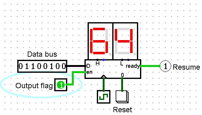
Output display is not as easy. It requires a register to store the output value and it should also work independently of the user so it needs to implement automatic handshaking: something that emits a "Ready" signal after receiving the in signal and storing data, and takes it down when the in signal ends.
Fortunately both are still quite simple to set up. The data register is just a standard register with its "enable" input connected to the in signal so that it only loads data when it's supposed to. The handshake can be performed by a one-byte register (AKA D-flip-flop): it will pass on the in signal as a resume signal but synchronised with the module's clock* and will be reset asynchronously when in goes down.
Outputs are set up for connection with Logisim's hex displays, so from the outside the whole setup looks like this:
Hex output module in use*In my final simulation everything will run on the same clock, but I want to design the BPU tot be able to communicate with devices with different speeds.
Conclusion
That's all, folks!
This week I've shown you a handshake protocol for communication between devices of different speeds and designed the external parts needed to operate the BPU. Next week I'll begin designing the BPU itself starting from some core registers.
This content originally appeared on DEV Community and was authored by Alex Esoposting
Alex Esoposting | Sciencx (2021-06-04T10:54:58+00:00) Input, output and memory for the BPU. Retrieved from https://www.scien.cx/2021/06/04/input-output-and-memory-for-the-bpu/
Please log in to upload a file.
There are no updates yet.
Click the Upload button above to add an update.


